Gigabyte GA-7PESH1: A Dual Processor Motherboard through a Scientist’s Eyes
Browsing through a manufacturer’s website can offer a startling view of the product line up. Such was the case when I sprawled through Gigabyte’s range, only to find that they offer server line products, including dual processor motherboards. These are typically sold in a B2B environment (to system builders and integrators) rather than to the public, but after a couple of emails they were happy to send over their GA-7PESH1 model and a couple of Xeon CPUs for testing. Coming from a background where we used dual processor systems for some serious CPU Workstation throughput, it was interesting to see how the Sandy Bridge-E Xeons compared to consumer grade hardware for getting the job done
In my recent academic career as a computational chemist, we developed our own code to solve issues of diffusion and migration. This started with implicit grid solvers – everyone in the research group (coming from chemistry backgrounds rather than computer science backgrounds), as part of their training, wrote their own grid and solver classes in C++ which would be the backbone of the results obtained in their doctorate degree. Due to the idiosyncratic nature of coders and learning how to code, some of the students naturally wrote classes were easily multi-threaded at a high level, whereas some used a large amount of localized cache which made multithreading impractical. Nevertheless, single threaded performance was a major part in being able to obtain the results of the simulations which could last from seconds to weeks. As part of my role in the group, I introduced the chemists to OpenMP which sped up some of their simulations, but as a result caused the shift in writing this code towards the multithreaded. I orchestrated the purchasing of dual processor (DP) Nehalem workstations from Dell (the preferred source of IT equipment for the academic institution (despite my openness to build in-house custom hardware) in order to speed up the newly multithreaded code (with ECC memory for safety), and then embarked on my own research which looked at off-the-shelf FEM solvers then explicit calculations to parallelize the code at a low level, which took me to GPUs, which resulted in nine first author research papers overall in those three years
In a lot of the simulations written during that period by the multiple researchers, one element was consistent – trying to use as much processor power as possible. When one of us needed more horsepower for a larger number of simulations, we used each other’s machines to get the job done quicker. Thus when it came to purchasing those DP machines, I explored the SR-2 route and the possibility of self-building the machines, but this was quickly shot down by the IT department who preferred pre-built machines with a warranty. In the end we purchased three dual E5520 systems, to give each machine 8 cores / 16 threads of processing power, as well as some ECC memory (thankfully the nature of the simulations required no more than a few megabytes each), to fit into the budget. When I left that position, these machines were still going strong, with one colleague using all three to correlate the theoretical predictions with experimental results
Since leaving that position and working for AnandTech, I still partake in exploring other avenues where my research could go into, albeit in my spare time without funding. Thankfully moving to a single OCed Sandy Bridge-E processor let me keep the high level CPU code comparable to during the research group, even if I don’t have the ECC memory. The GPU code is also faster, moving from a GTX480 during research to 580/680s now. One of the benchmarks in my motherboard reviews is derived from one of my research papers – regular readers of our motherboard reviews will recognize the 3DPM benchmark from those reviews and in the review today, just to see how far computation has gone. Being a chemist rather than a computer scientist, the code for this benchmark could be comparable to similar non-CompSci trained individuals – from a complexity point of view it is very basic, slightly optimized to perform faster calculations FMA but not the best it could be in terms of full blown SSE/SSE2/AVX extensions et al
With the vast number of possible uses for high performance systems, it would be impossible for me to cover them all. Johan de Gelas, our server reviewer, lives and breathes this type of technology, and hence his benchmark suite deals more with virtualization, VMs and database accessing. As my perspective is usually from performance and utility, the review of this motherboard will be based around my history and perspective. As I mentioned previously, this product is primarily B2B (business to business) rather than B2C (business to consumer), however from a home build standpoint, it offers an alternative to the two main Sandy Bridge-E based Xeon home-build workstation products in the market – the ASUS Z9PE-D8 WS and the EVGA SR-X. Hopefully we will get these other products in as comparison points for you
Visual Inspection
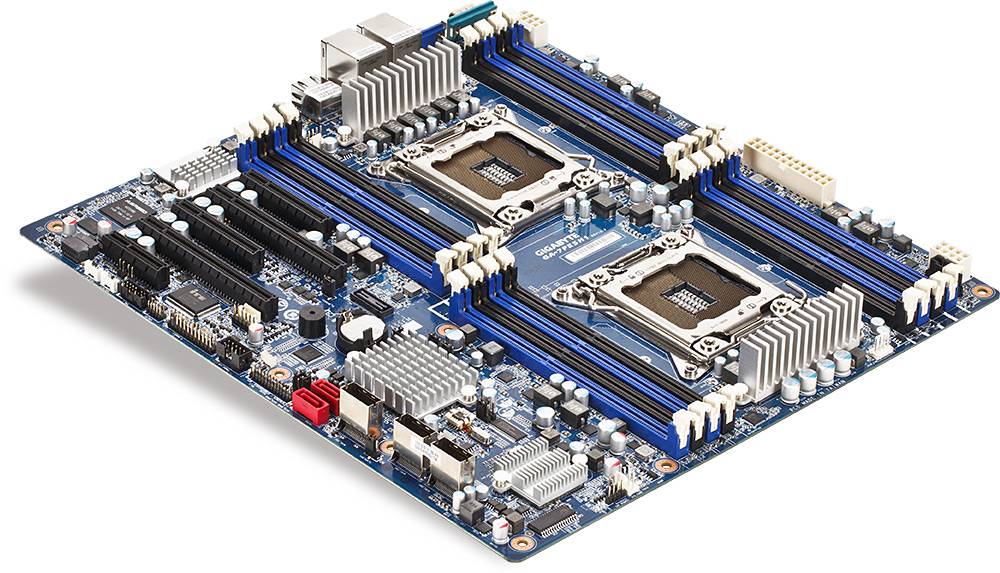
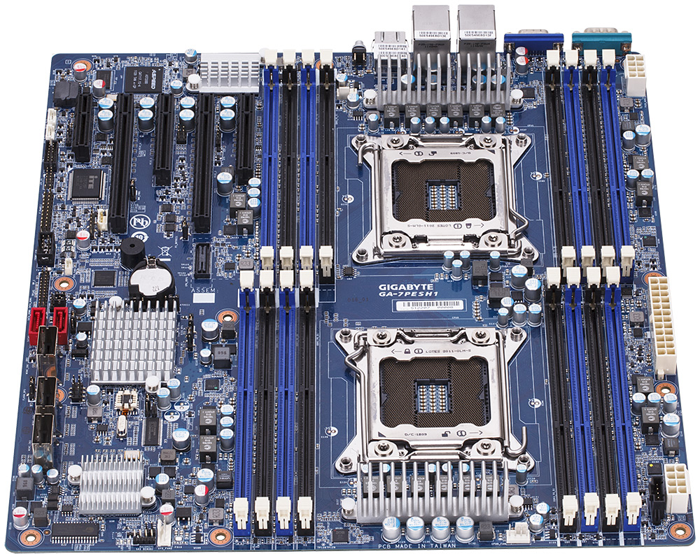
I knew server boards were large, but coming from the ATX and E-ATX standards, this thing is huge. It measures 330mm x 305mm (13” x 12”) which correlates to the SSI EEB specification for server motherboards. This is the size exact size of an official E-ATX motherboard (despite a small amount of loose definition), but to put the icing on the cake, the mounting holes for the motherboard are different to the normal ATX standards. If we took a large case, like the Rosewill Blackhawk-Ultra, it supports ATX, SSI CEB, XL-ATX, E-ATX and HPTX, up to 13.6” x 15”, but not SSI EEB. Thus drilling extra holes for standoffs may be required
Unlike the SR-X or Z9PE-D8 WS, the GA-7PESH1 supports two memory modules per channel for all channels on board. In terms of specifications this means support for up to 128 GB UDIMM (i.e. regular DDR3), 128 GB UDIMM ECC, and 512 GB RDIMM ECC. Due to the nature of the design, only 1066-1600 MHz is supported, but the GA-7PESH1 supports 1600 MHz when all slots are populated. For our testing, Kingston has kindly supplied us with 8x4GB of their 1600 C11 ECC memory
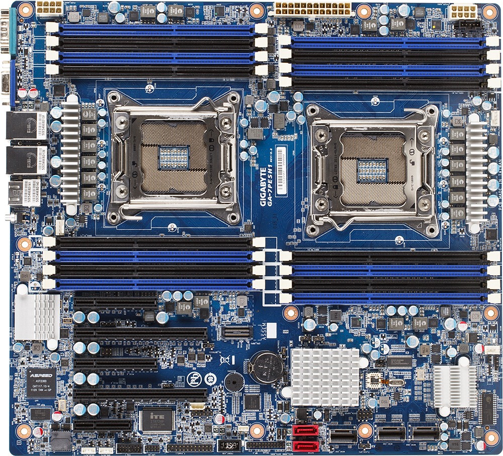
As with the majority of server boards, stability and longevity is a top priority. This means no overclocking, and Gigabyte can safely place a six phase power delivery on each CPU – it also helps that all SB-E Xeons are multiplier locked and there is no word of unlocked CPUs being released any time soon. As we look at the board, standards dictate that the CPU on the right is designated as the first CPU. Each CPU has access to a single fan header, and specifications for coolers are fairly loose in both the x and the y directions, limited only by memory population and the max z-height of the case or chassis the board is being placed into. As with all dual CPU motherboards, each CPU needs its own Power Connector, and we find them at the top of the board behind the memory slots and at opposite ends. The placement of these power connectors is actually quite far away for a normal motherboard, but it seems that the priority of the placement is at the edge of the board. In between the two CPU power connectors is a standard 24-pin ATX power connector
One of the main differences I note coming from a consumer motherboard orientation is the sheer number of available connectors and headers on such a server motherboard. For example, the SATA ports have to be enabled by moving the jumpers the other side of the chipset. The chipset heatsink is small and basic – there is no need for a large heatsink as the general placement for such a board would be in a server environment where noise is not particularly an issue if there are plenty of Delta fans to help airflow
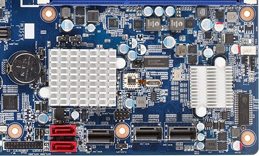
On the bottom right of the board we get a pair of SATA ports and three mini-SAS connections. These are all perpendicular to the board, but are actually in the way of a second GPU being installed in a ‘normal’ motherboard way. Users wishing to use the second PCIe x8 slot on board may look into PCIe risers to avoid this situation. The heatsink on the right of this image covers up an LSI RAID chip, allowing the mSAS drives to be hardware RAIDed
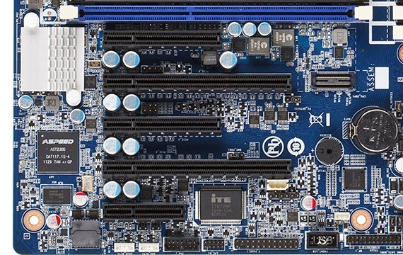
As per normal operation on a C602 DP board, the PCIe slots are taken from the PEG of one CPU. On some other boards, it is possible to interweave all the PCIe lanes from both CPUs, but it becomes difficult when organizing communication between the GPUs on different CPUs. From top to bottom we get an x8 (@x4), x16, x8 (@x4), x16 (@x8), x4(@x1). It seems odd to offer these longer slots at lower speed ratings, but all of the slots are Gen 3.0 capable except the x4(@x1). The lanes may have been held back to maintain data coherency
To those unfamiliar with server boards, of note is the connector just to the right of center of the picture above. This is the equivalent of the front panel connection on an ATX motherboard. At almost double the width it has a lot more options, and where to put your cables is not printed on the PCB – like in the old days we get the manual out to see what is what
On the far left we have an ASPEED AST2300 chip, which has multiple functions. On one hand it is an onboard 2D graphics chip which powers the VGA port via its ARM926EJ (ARM9) core at 400 MHz. For the other, it as an advanced PCIe graphics and remote management processor, supporting dual NICs, two COM ports, monitoring functions and embedded memory. Further round this section gives us a removable BIOS chip, a COM header, diagnostic headers for internal functions, and a USB 2.0 header
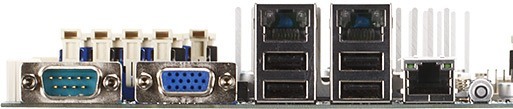
The rear IO is very bare compared to what we are normally used to. From left to right is a serial port, the VGA port, two gigabit Ethernet NICs (Intel I350), four USB 2.0 ports, the KVM server management port, and an ID Switch button for unit identification. There is no audio here, no power/reset buttons, and no two-digit debug LED
